C101A has an over voltage protection circuit for the first stage FET, so you do not need to be too concerned about the time change of the bias voltage when turning it on and off (however, you should be careful not to exceed the voltage limit (= ±500 V)).
To demonstrate the above, a high voltage application test was carried out using the configuration shown in Figure 1.

Figure 1 Test configuration
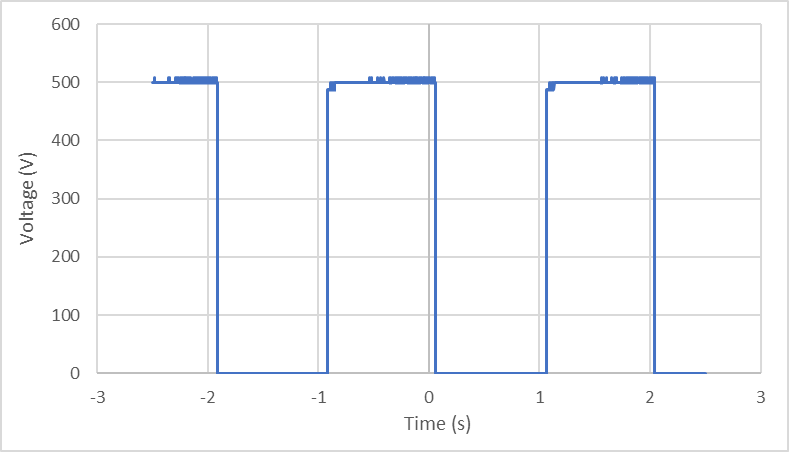
The high voltage was applied directly to the input connector electrode of the C101A. In normal measurements, a detector is placed between the high voltage power supply and the input connector, but in this case, a direct connection is used to ensure at the severer conditions. The same reason is why the bias voltage input of the C101A is not used. The actual voltage waveform is shown in Figure 2.

Figure 2 Voltage waveform observed at the oscilloscope
where, the rise time (10% to 90%) of the voltage waveform in Figure 2 is 1 ms, and the fall time (90% to 10%) is 0.5 ms.
As shown in Figure 2, the voltage was switched 1000 times (required time: about 2000 seconds) between +500 V and 0 V at 1 second intervals. During this time, the power supply of the C101A was on (= supplying ±12 V).
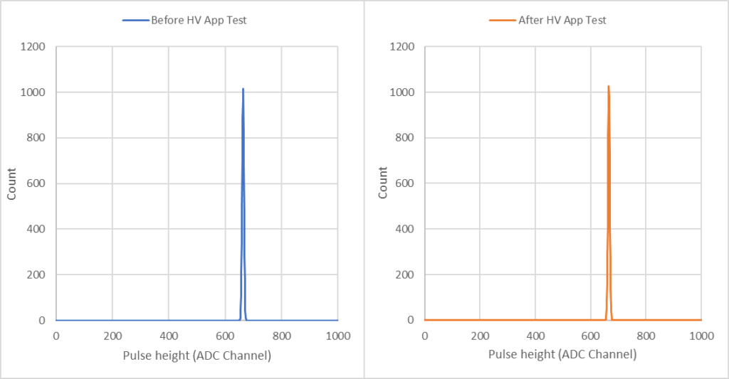
After this test, no malfunctions were observed in the C101A. Figure 3(a)(b) shows the spectrum of the test pulse before and after the test. You can see that the performance has not changed.

(a) Before the test (b) After the test
Figure 3 Spectrum of test pulse before and after the test
In addition, C102A uses the same circuitry as C101A, thus the same would be expected to C102A.